JTAG Interface
JTAG Bus Description
IEEE Std 1149.1-1990 JTAG (Joint Test Action Group); Test Access
Port and Boundary-Scan Architecture. This is a serial bus with four
signals: Test Clock (TCK), Test Mode Select (TMS), Test
Data Input (TDI), and Test Data Output (TDO). The bus is used
as a test bus for the 'Boundary-Scan' of ICs, as in
Design-For-Testability (DFT). To use JTAG, during the design, you most
select JTAG compatible devices. ICs supporting JTAG will have the four
additional pins listed above. Devices reside on the bus in a daisy chain,
with TDO of one device feeding TDI of the next device. In addition to
having the pins listed above each device most have a Boundary-Scan
Register. The Boundary-Scan Register may be used to test the
interconnection between ICs [Chip-to-Chip] or test with in the IC.
Boundary-scan tests can be used to check continuity between devices.
Continuity checks on PWB nets may be performed by sending out a know
pattern and receiving that same pattern at the input to another IC(s).
Not receiving the test signal or pattern would indicate a broken PWB
trace, a failed IC, or cold solder joint.
|
TCK: [Test Clock] has noting to do with the board or system clock.
The Test Clock is used to load the test mode data from the TMS pin, and
the test data on the TDI pin [on the rising edge]. On the falling edge
test clock outputs the test data on the TDO pin. As with any clock pin
this line needs to be terminated in order to reduce reflections. The termination should be a 68 ohm resistor in series with a 100pF capacitor to ground. The TCK signal is bused to all Integrated Circuits [IC] in the JTAG chain. The signal may require buffering or be fanned out by multiple drivers depending on the distance and number of devices in the chain. Using multiple drivers would also require a termination resistor on each TCK line.
TMS: [Test Mode Select Input] controls the operation of the test
logic, by receiving the incoming data]. The value at the input on the
rising edge of the clock controls the movement through the states of the
TAP controller. The TMS line has an internal pull-up, so the input is
high with no input. The TMS signal is bused to all ICs in the JTAG chain. The TMS line should have a 10k pull-up resistor on the line.
TDI: [Test Data Input] receives serial input data which is either
feed to the test data registers or instruction register, but depends on
the state of the TAP controller. The TDI line has an internal pull-up, so
the input is high with no input. The TDI signal is feed to the TDI pin of the first IC in the JTAG chain. The TDO signal from that IC is then sent to the TDI pin of the next IC in the chain or sent back out to the JTAG header. The TDI line should have a 10k pull-up resistor on the line.
TDO: [Test Data Output] outputs serial data which comes from
either the test data registers or instruction register, but depends on
the state of the TAP controller. Data applies to the TDI pin will appear
at the TDO pin but may be shifted of a number of clock cycles, depending
on the length of the internal register. The TDO pin is
high-Impedance. The TDO signal is the output from a JTAG device that feed the TDI input of another JTAG device. The TDO line should have a 10k pull-up resistor on the line. The TDO signal should also include a 22 ohm series resistor placed near the last device in the JTAG chain.
TRST: [Test Rest] will asynchronously reset the JTAG test logic.
The logic is reset (with TRST) regardless of the state of TMS or TCLK. The TRST signal is bused to all ICs in the JTAG chain. The TRST signal should include a pull-down resistor when possible to reduce the chance the signal floats.
|
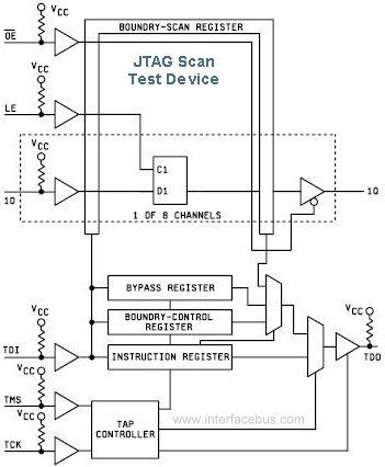
IEEE-1149 JTAG Scan Device
|
20 Pin JTAG Pin Out
| Pin |
Function |
Pin |
Function |
| 1 |
TRST |
2 |
GND |
| 3 |
TDO |
4 |
GND |
| 5 |
TDI |
6 |
GND |
| 7 |
TMS |
8 |
GND |
| 9 |
TCK |
10 |
GND |
| 11 |
VPP_E |
12 |
GND |
| 13 |
A/W |
14 |
GND |
| 15 |
User 0 |
16 |
GND |
| 17 |
Rdy/Bsy |
18 |
GND |
| 19 |
User 1 |
20 |
Vcc |
In many cases the JTAG connector is a simple two row header on a center-line of 0.100 inches [pin-to-pin spacing].
Header -- A ten pin header is also common, using signal 1 to ten in the same configuration shown above.
The TCLK signal should be terminated to match the trace impedance [cable]
in high speed applications. A capacitor may be placed in series with the
termination resistor to reduce loading of the resistor. A series resistor
may be used in line with the TDO signal to damp out reflections. The TDO
series resistor should be used after the last device in the chain and
before the TDO [exit] pin. All other JTAG lines should be pulled high via
a resistor. The pull-up resistor is designed to provide a weak pull-up so
a value around 10k will be adequate. Standard design rules apply to the
JTAG pins and include requirements to buffer the signals if
required.
Note. BSDL [Boundary Scan Description Language] is a subset of the
VHDL standard.
Any manufacturer of a JTAG compliant device must provide a BSDL file for
that device. The BSDL file contains information on the function of each
of the pins on the device - which are used as I/Os, power or ground. BSDL
files describe the Boundary Scan architecture of a JTAG-compliant device,
and are written in VHDL. The BSDL file includes:
... 1. Entity Declaration: The entity declaration
is a VHDL construct that is used to identify the name of the device that
is described by the BSDL file.
... 2. Generic Parameter: The Generic parameter specifies which
package is described by the BSDL file.
... 3. Logical Port Description: lists all of the pads on a
device, and states whether that pin is an input(in bit;), output(out
bit;), bidirectional (inout bit;) or unavailable for boundary scan
(linkage bit;).
... 4. Package Pin Mapping: The Package Pin Mapping shows how the
pads on the device die are wired to the pins on the device package.
... 5. Use statements: The use statement calls VHDL packages that
contain attributes, types, constants, etc. that are referenced in the
BSDL File.
... 6. Scan Port Identification: The Scan Port Identification
identifies the JTAG pins: TDI, TDO, TMS, TCK and TRST (if used).
... 7. TAP description: provides additional information on the
device's JTAG logic; the Instruction Register length, Instruction
Opcodes, device IDCODE, etc. These characteristics are device
specific.
... 8. Boundary Register description: provides the structure of
the Boundary Scan cells on the device. Each pin on a device may have up
to three Boundary Scan cells, each cell consisting of a register and a
latch.
IEEE Std 1149.5-1995 IEEE Standard for Module Test and Maintenance
Bus (MTM-Bus) Protocol
Specifies a serial, backplane, test and maintenance bus (MTM-Bus).....
between a Test Control Master and up to 250 Slave modules.
The interface has 5 signals:
... MTM Clock (MCLK)
... MTM Control (MCTL)
... MTM Master Data (MMD)
... MTM Slave Data (MSD)
... MTM Pause Request (MPR).
This specification is
used at the Board level while 1149.1 is used at the chip level.
IEEE Std 1532 Boundary-Scan-based In System Configuration of
Programmable Devices; is a follow on or extension to JTAG.
IEEE std 1532 is a superset of the IEEE 1149.1 JTAG standard. IEEE 1532 also
provides additional flexibility for configuring
Programmable Logic Devices [FPGA, PLDs].
IEEE 1149 Standards:
IEEE 1149.1 deals with test for digital assemblies
IEEE 1149.4 deals with test for mixed signal and analog
assemblies
IEEE 1149.5 deals with test at system level
IEEE 1149.6 deals with requirements of boundary-scan testing of AC-coupled,
differential nets.
IEEE 1532 is a derivative standard for in-system programming of
digital devices
Note; although I sometimes list the date as part of the standard number [i.e. IEEE Std 1149.1-1990]
That does not imply that is the latest version; for example, IEEE Std 1149.1-2001 is the latest version.
Normally standards are revisited every five years.
Definitions:
ATE: Automatic Test Equipment
BIST: Built-In-Self-Test
BIT: Built-In-Test
BSDL: Boundary Scan Description Language
BSR: Boundary Scan Register
CBIT: Continuous BIT
DFT: Design-For-Test
JTAG: Joint Test Action Group
IBIT: Initiated BIT
IC: Integrated Circuit
ICT: In Circuit Test
PBIT: Power-up BIT
Altera ByteBlaster II Pin Out, Signal Assignments
10 Pin Altera ByteBlaster II
| Pin |
Function |
Pin |
Function |
| 1 |
TCK |
2 |
GND |
| 3 |
TDO |
4 |
Power |
| 5 |
TMS |
6 |
NC |
| 7 |
NC |
8 |
NC |
| 9 |
TDI |
10 |
GND |
Xilinx Cable IV Pin Out, Signal Assignments
14 Pin Xilinx Cable IV
| Pin |
Function |
Pin |
Function |
| 1 |
VGND |
2 |
VREF |
| 3 |
GND |
4 |
TMS |
| 5 |
GND |
6 |
TCK |
| 7 |
GND |
8 |
TDO |
| 9 |
GND |
10 |
TDI |
| 11 |
GND |
12 |
NC |
| 13 |
GND |
14 |
NC |
JTAG target system ports may be JTAG, E-JTAG, OnCE, COP, BDM, or something else.
DOD Drawing Number: 5962-91725; Scan Test Device with Octal D-Type Latch Three state Outputs [54BCT8373A]
DOD Drawing Number: 5962-91726; Scan Test Device with Octal Buffer Three state Outputs [54BCT8244A]
DOD Drawing Number: 5962-91727; Scan Test Device with Octal D-Type Edge Triggered Flip-Flop Three state Outputs [54BCT8374A]
DOD Drawing Number: 5962-91728; Scan Test Device with Octal Bus Transceiver Three state Outputs [54BCT8245A]
DOD Drawing Number: 5962-93228; Test Bus Controller, Digital, CMOS, Microcircuit [54ACT8990]
Modified 8/4/11
Copyright © 1998 - 2011 All rights reserved Leroy Davis


